2024-04-20 Saturday

Time:2020-11-11 Reading:11739
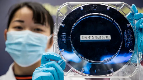
On October 16th, the 2020 China
International Graphene Innovation Conference was held, where new materials such
as ultra-flat copper-nickel alloy single-crystal wafers, 8-inch graphene
single-crystal wafers, and germanium-based graphene wafers were unveiled,
showcasing China's innovative achievements in high-quality graphene materials.
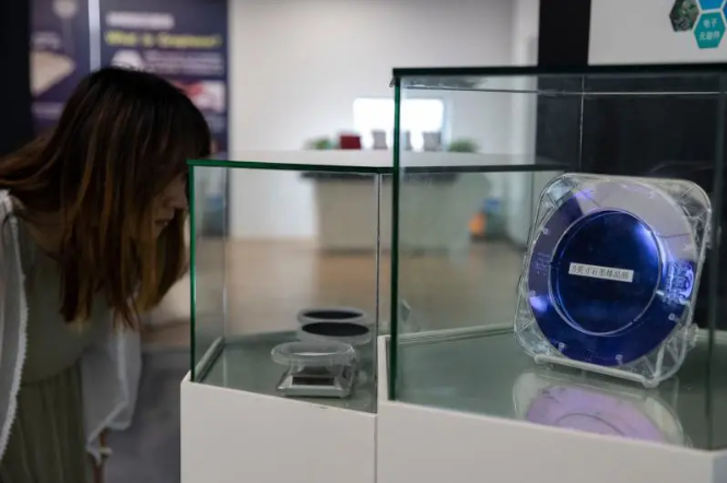
Driven by the Shanghai Graphene Industry Technology Functional Platform, the
research team has achieved small-batch production of these achievements,
leading internationally in terms of product size and quality.
In 2009, the research team from the
Shanghai Institute of Microsystem and Information Technology, Chinese Academy
of Sciences, targeted the key issues in the preparation of graphene single
crystals and their applications in electronic devices, embarking on tackling
these challenges. "Just like the material for manufacturing silicon chips
is silicon single-crystal wafers, if you want to use graphene and other
carbon-based two-dimensional materials to achieve integrated electronic
devices, initiating a revolution in microelectronics technology, you must
prepare large size, high-quality graphene single-crystal wafers," said Wu
Tianru, Associate Researcher of the Institute.
It can be said that after ten years
of hard work, with the support of major national scientific and technological
projects and Shanghai Science and Technology Innovation Action Plan projects,
the research team aimed at the high ground of high-quality graphene preparation
and high-performance device technology. They focused on the controllable
preparation of wafer-level graphene single crystals, concentrating on the
development and expansion of new functions and applications of graphene. From
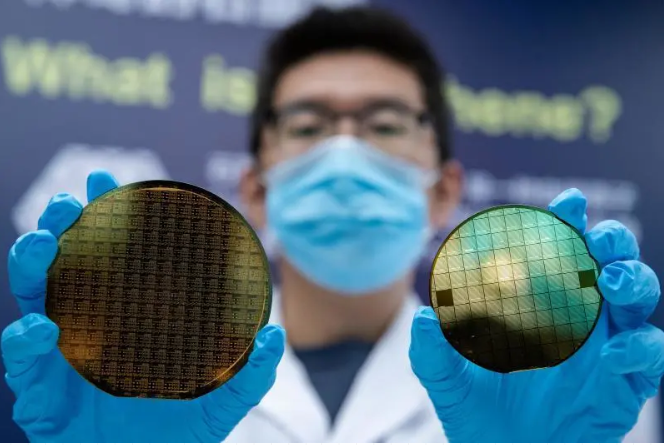
growing monolayers to single crystals, and then to atomically flat large-area
wafers, Shanghai scientists have finally upgraded graphene from samples of a few
micrometers peeled off with tape to 8-inch wafers that can be produced on a
large scale.
To realize the mass production of
graphene wafers as soon as possible, the Shanghai Institute of Microsystem and
Information Technology, Chinese Academy of Sciences, signed an agreement with
the Shanghai Graphene Functional Platform last September, offering
cost-competitive industrial applications. Moreover, atomically thin graphene
materials can act as powerful sensors for various physical parameters (chemical
composition, humidity, temperature, strain, etc.). These single-chip sensing
platforms, combined with radio frequency identification antennas, can be used
as remotely readable detectors.
The small-batch production of
graphene wafers has laid the foundation for the research and development of a
new generation of domestic electronic devices. At present, some electronic
components based on graphene and used for data communication are undergoing
prototype demonstrations in the industry. Among them, electronic and photonic
components have been integrated into transmission systems and validated,
achieving high-speed, low-power data or telephone communications. The
optoelectronic modules of graphene photodetectors can detect the entire band
from visible light to thermal ranges. Under the CAS and China Electronics
Group, breakthroughs have been made in the core processes of graphene terahertz
detector devices, high-performance radio frequency transistors, and other
electronic devices using Shanghai research materials.
Article
transferred from WeChat Public Account "Shanghai Science and
Technology".
TEL:021-37896100
EMAIL:icti@shicti.com
ADDRESS:Building 11, No. 300, Dingyuan Road, Songjiang District, Shanghai

沪ICP备19009172号-3Copyright © 上海簇睿低碳能源技术有限公司 All Rights Reserved.